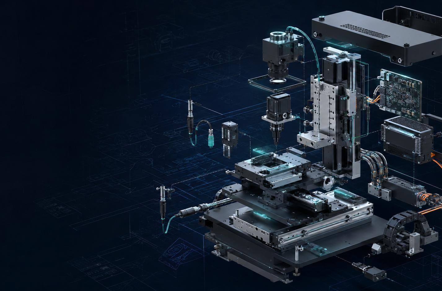
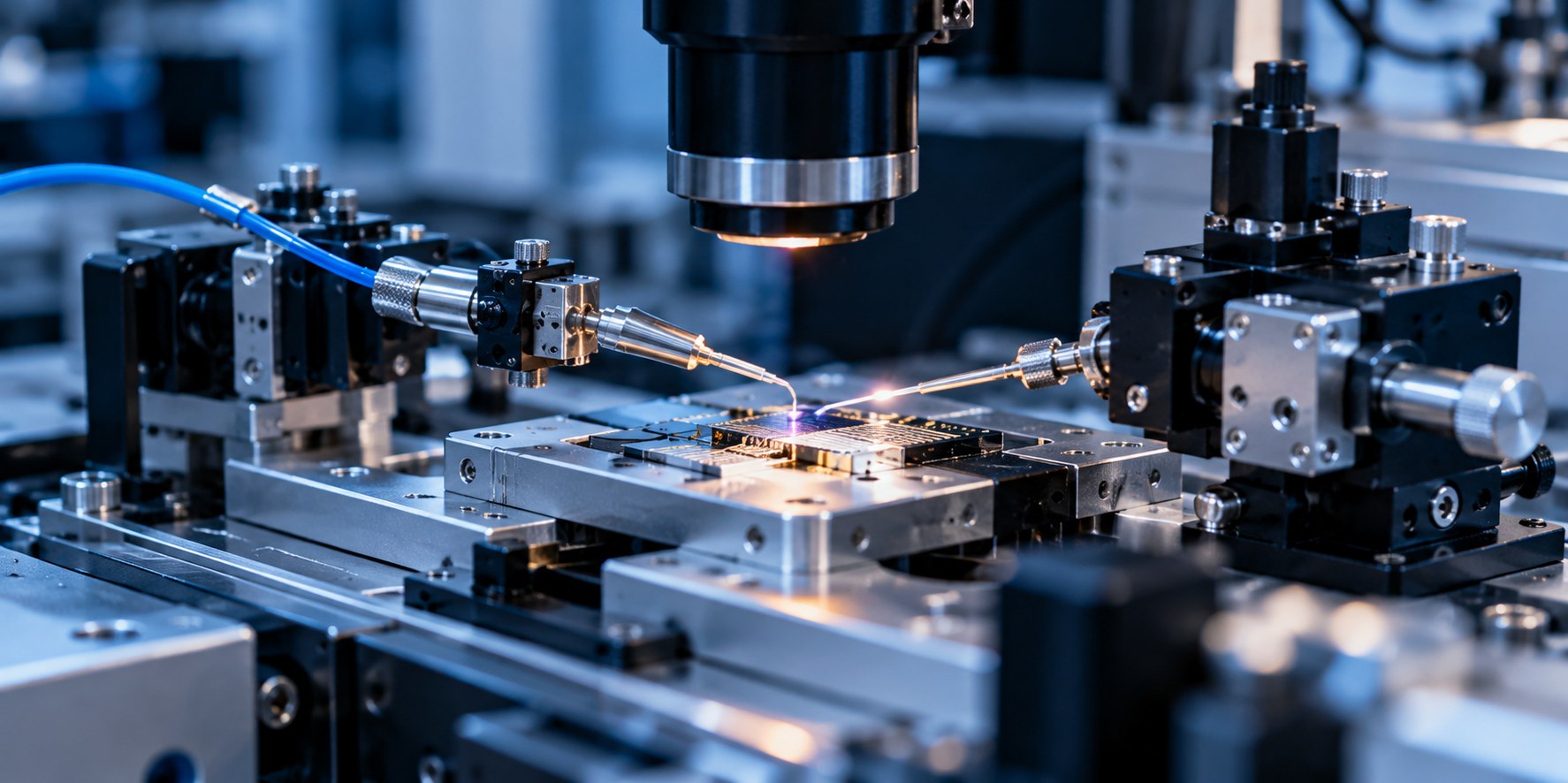
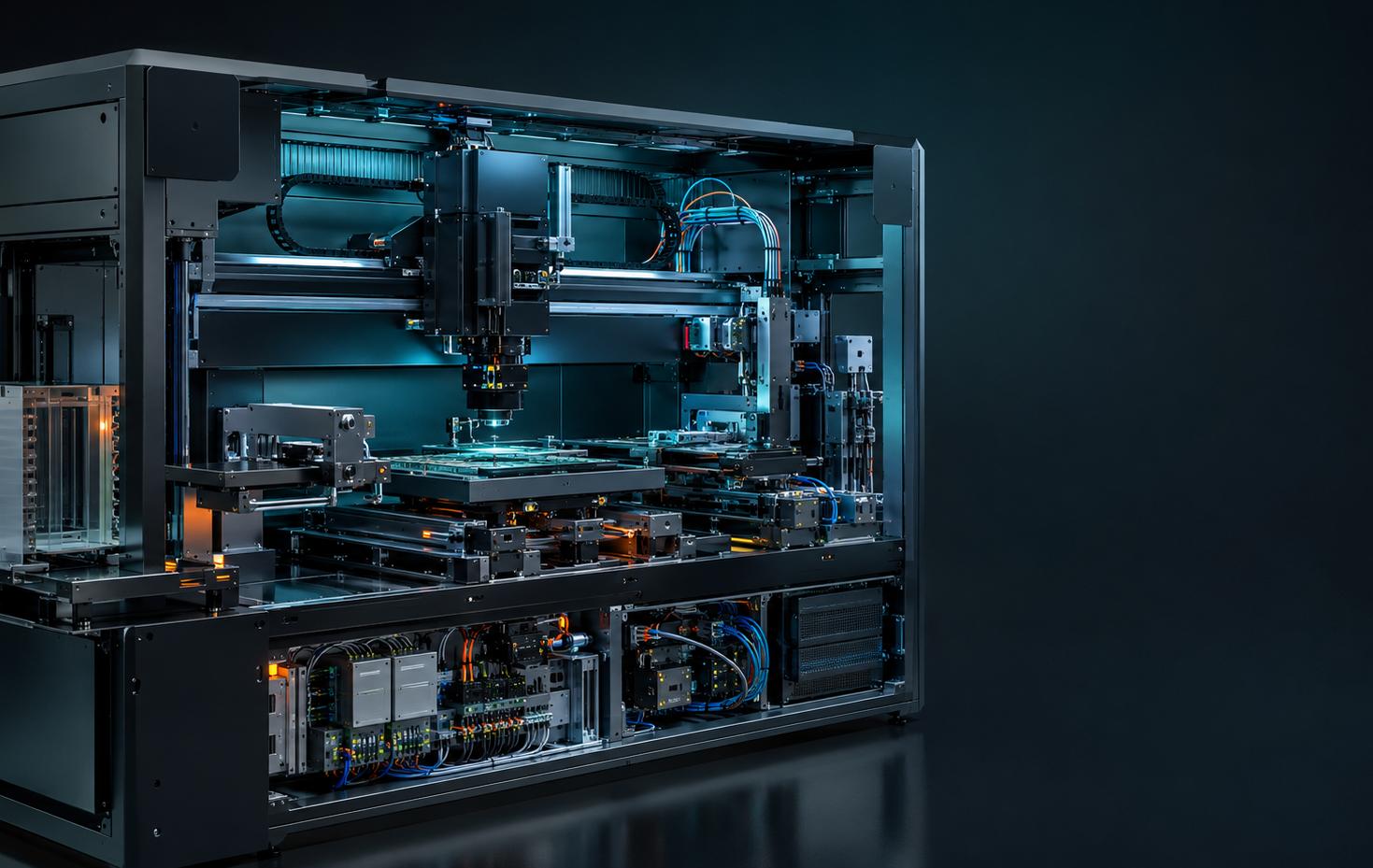
Automated Receptacle Alignment System (Photonics Alignment)
Sub-micron active fiber-to-chip and laser-to-PIC automated coupling.
 ST Semiconductor Testing Pte. Ltd.
Precision equipment and specialized engineering services for the semiconductor and photonics ecosystem.
Sub-micron active fiber-to-chip and laser-to-PIC automated coupling.
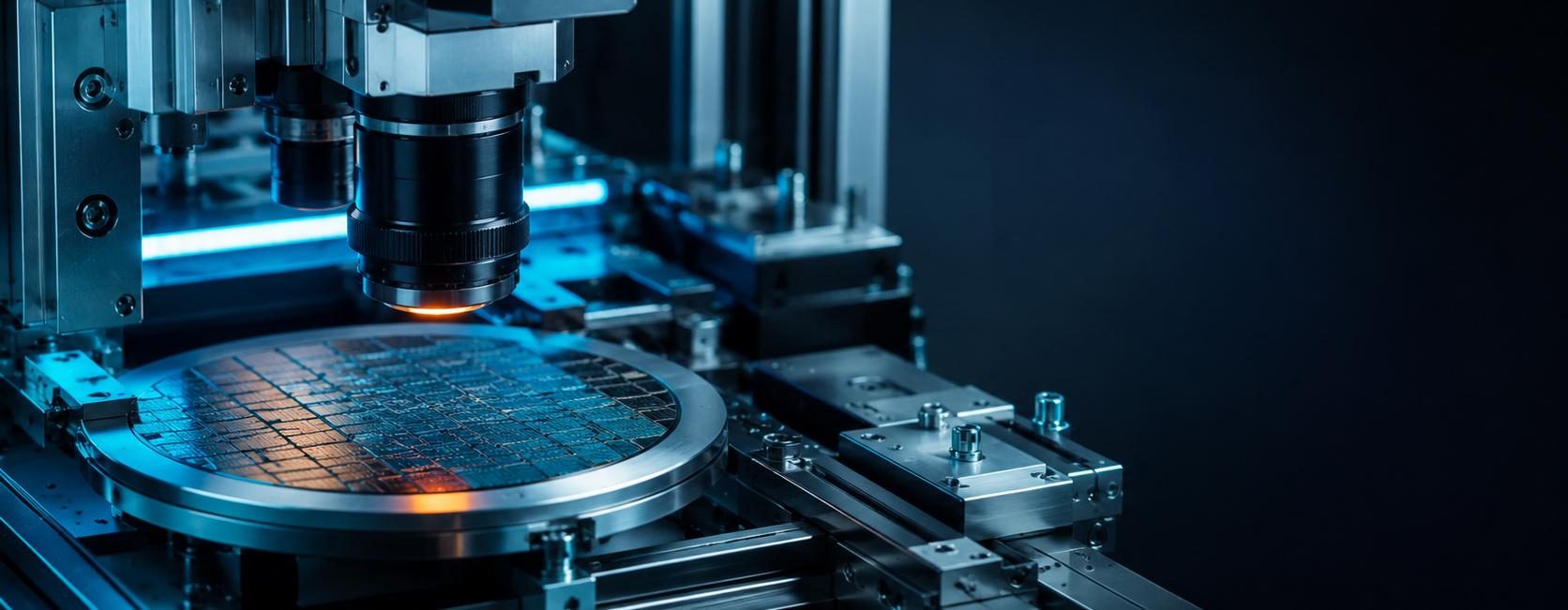
Equipment for advanced 2.5D and 3D semiconductor integration.

Wafer-level and chip-level testing and characterization solutions.

Vision-driven surface and defect inspection systems.

Custom test development, characterization and pilot solutions.
Application-specific tooling, modules and engineering support.
Our engineering disciplines cover mechanical design, controls, software, machine vision, precision motion, system integration, manufacturing and testing.